If you already have a chip design and want to make a nice rendering of how it will look when fabricated, this can easily be done easily with a raster export of the layout and some simple shaders in Blender. This post assumes some familiarity with Blender.
Open up your chip design (here I’m using KLayout), set the background to black and make sure any grids are hidden. Then, set any metal layers to colors that wouldn’t look out of place on a wafer (blues, grays, etc.).
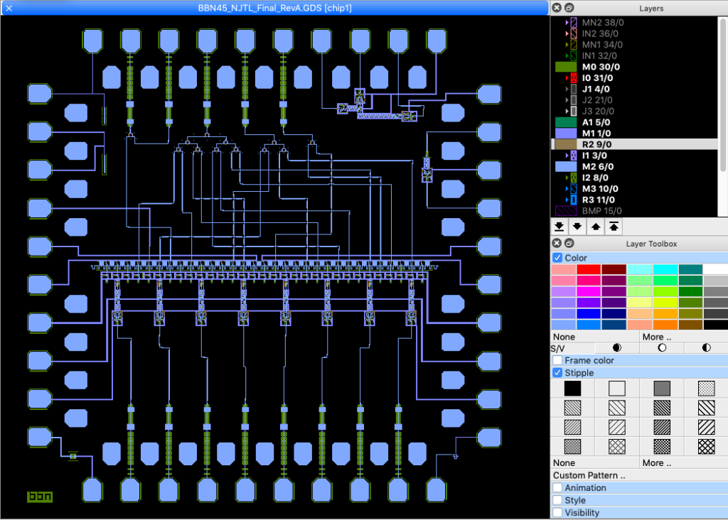
Next, take a screenshot of the layout. If you want to make close-up renders the resolution will likely need to be higher than your native screen resolution — luckily one can use a simple KLayout macro to take a screenshot with arbitrary resolution. Something like 4000×4000 should be sufficient for most purposes. In a later post we will perform a vector export and try to reconstruct realistic 3D geometry.
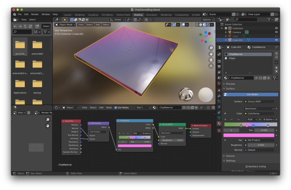
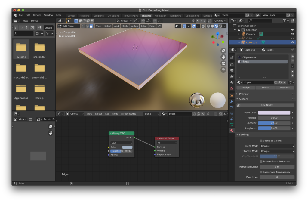
Next, fire up Blender (using version 2.90 here) and scale the default cube to match the dimensions of your chip using the dimensions in the transform panel (press “N” to bring up the tools tab).
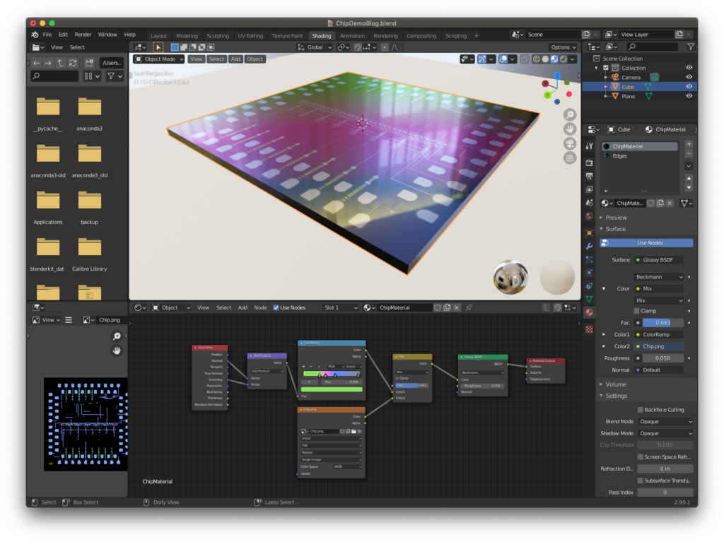
Create a new material called ChipMaterial (using nodes) and implement something similar to the following. We take the dot product between the face normal and the ray heading towards the camera, which gives the cosine of the incident light angle assuming a glossy surface. The ColorRamp node approximates the viewing-angle dependence of the dielectric color, you can play with these values to meet your aesthetic requirements. Using a B-spline interpolation eUse a low roughness and a Glossy BSDF shader for the surface output.
Create a second material slot with a simple glossy shader and use a higher roughness value for the chip edges. In edit mode, select the faces at the edge of the chip and assign your edge material to them so they don’t have the gradient from the surface dielectric.
Next, we mix the image texture we’ve exported into KLayout into the output of the ColorRamp node for ChipMaterial. You can do more complex things to blend the textures, but changing the mixing factor gives acceptable results. Using some clamping and ramping you can even add a fake process bias to your “lithography”! If you texture is distorted, select the top of the chip in edit mode and press “U” for the UV Editing menu followed by “Unwrap”. If there is still extra space around your chip you can edit the UV map with this top face selected and scale the UV until it properly brackets your screenshot from earlier.
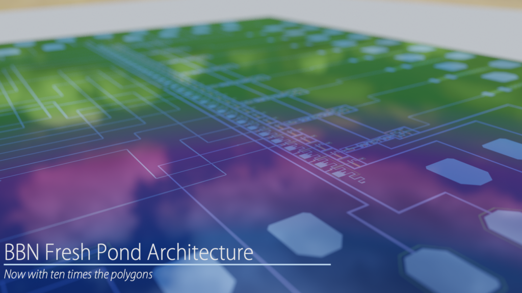
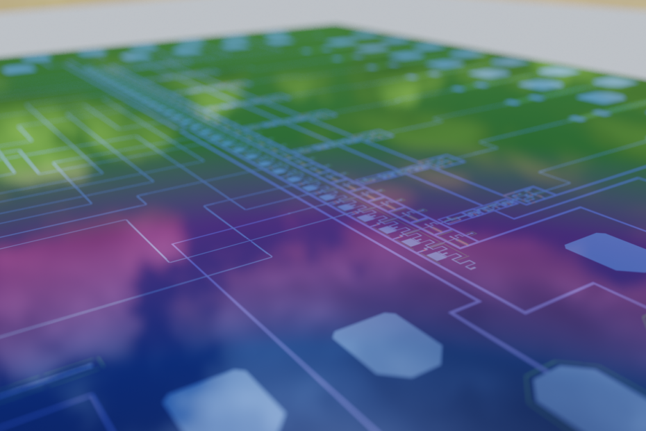
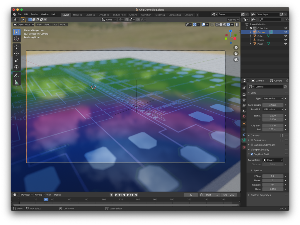
Now it just remains to make things look more realistic. Add a plane under the chip (already shown above) and add a high resolution HDRI as the environment texture for the “world.” Forgive me for using something with clouds here — I haven’t found many HDRIs of clean rooms. I changed the rendering engine to Cycles and then tweaked the intensity of the world background to 2–3 to give a reasonable lighting level. Next I added an empty, and focused the camera on the empty enabled depth of field with a low f-stop of 0.2. I changed the focal length to 32 mm and then used the tilde key “~” and and the WASD+QE keys to fly the camera around until I was bracketing some interesting portion of the circuit.
There’s not much left to do at this point. Do a render and slap it in a slide deck!